0-2 GHz All-band, All-mode Transmit & Receive Converter
Converts any HF radio to any amateur band - 136 kHz through 1296 MHz better than 1 Hz frequency accuracy
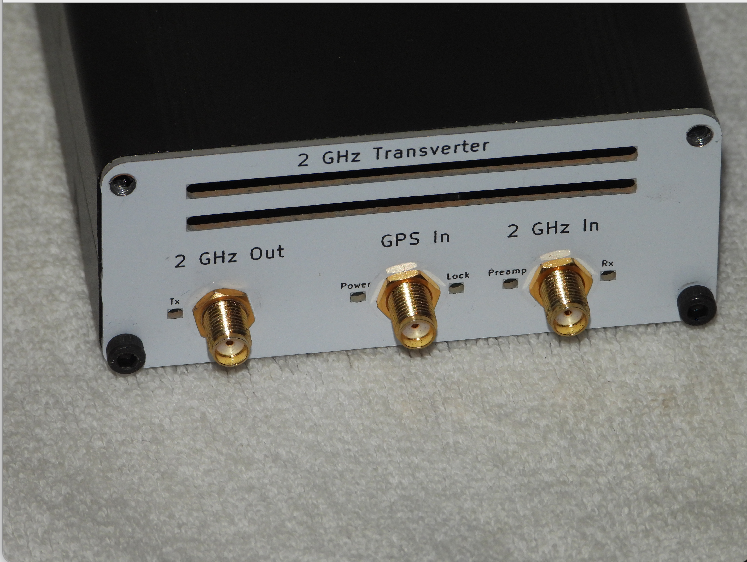
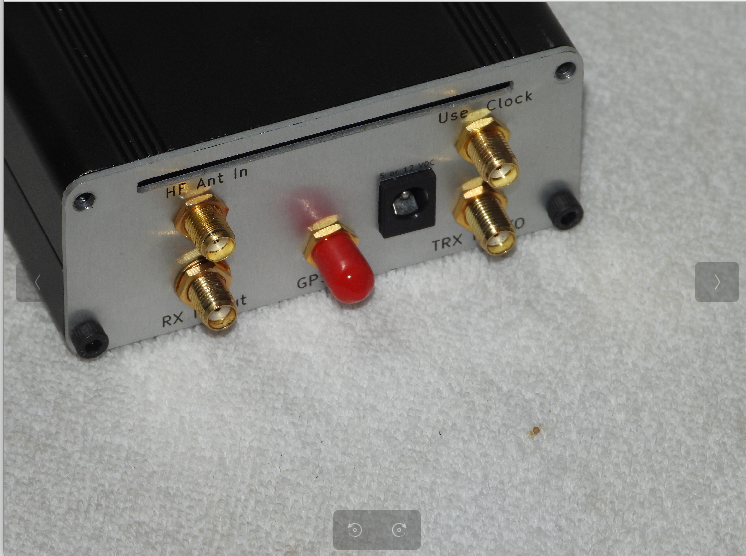
Features
Web Interface
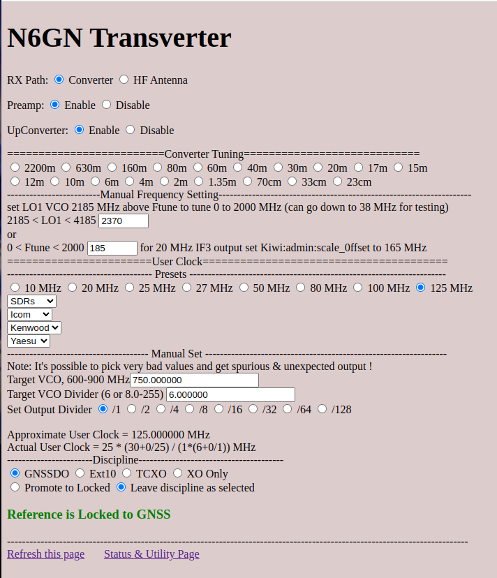
How It Works
Simple conversion techniques involve an offsetting oscillator and a mixer. For typical passive mixers, conversion is symmetrical so it can be performed either lower frequency to higher or the other way around. But the conversion/mixing process is nonlinear and generates more than a single output. There are image frequency, harmonic mixing and harmonics of the signal and of the local oscillator (LO) present at the output. For simple systems filtering, balance and other steps need to be taken to assure a single frequency is converted without generation of unwanted signals.
This transverter uses a triple conversion technique to remove many of the unwanted signals that are present in a simple conversion process. It does this by generating an intermediate frequency which is above the highest range of desired frequencies along with a low pass filter to remove image frequency, LO and other unwanted components. It offers the ability to quickly tune one of the conversion LOs to produce a desired output over a wide range of offsets.
For this transverter the goal is to convert the operation of an amateur radio HF transceiver or transmitter/receiver combination to and from any frequency from near-DC to 2 GHz. The triple conversion method shown along with a disciplined LO system which is common to both transmit and receive conversion is used to generate accurate copies of an incoming/receive signal to an HF intermediate frequency (IF) between 10-30 MHz while a symmetrical process is used to simultaneously convert an HF transmitting IF to the same range.
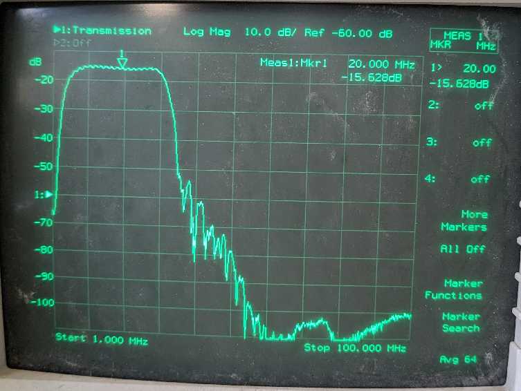
The following plot is a vector network analyzer (VNA) measurement of the transmit side of the transverter in action. Because without extra effort the VNA cannot measure frequency converted signals, that is, the stimulus and sensed signal must be at the same frequency as the detected signal within the VNA, to make this measurement the transverter was tuned to produce no net frequency conversion; the offsetting frequency was set to zero. With this done, both the receive and transmit conversion paths can be measured. The measurement was taken with 30 dB of extra attenuation and shows the transmit converter flatness and about 14 dB of conversion gain where the output power was about +13 dBm or 20 mW.
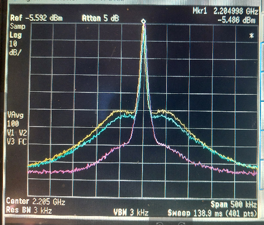
Phase noise performance of the three LO's give a good approximation of end performance. All LO's are referenced to the same clock
Complete Stations
Transverter in use to convert an Icom IC7300 for use on 70cm NBFM. A Transceiver Interface conditions the Icom input/output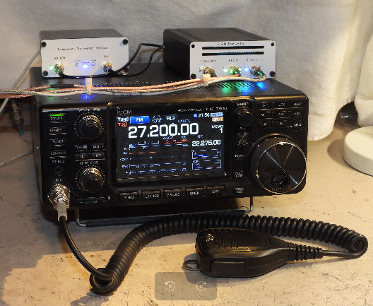
Final
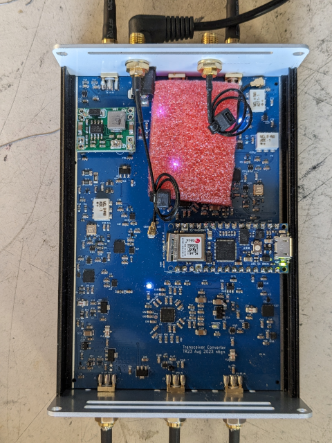
Assembly & Test
After receiving assembled PCB from fabrication and before final assembly with the CPU & socket, first verify with an ohmmeter that the power input line and the 5V and 3V regulator outputs are not shorted. Next connect a current limited or low power source of 7-16 VDC power the board. Without CPU verify that there is only a few mA flowing. The raw PCBs have already been pretested but doing this makes sure nothing has gone wrong during component assembly or soldering.
|
||||
Item Description |
Provider |
Source Code |
Notes |
Approximate Material Cost(excludes setup fees and shipping) |
Assembled Transverter PCB |
DownloadTRansverter Kit Files |
Download TRansverter PCB Source |
US$190 | |
| IoT33 CPU |
Arduino Store |
US$26 | ||
| 2 x 15p CPU socket |
eBay |
US$2 | ||
120x88x38mm Clamshell Enclosure
|
JLCMC
|
Much more economical than previous eBay sources | US$3 |
|
88x38mm Front Panel |
Download TRFront Panel Kit |
Download TR Front Panel Source |
US$1 |
|
88x38mm Rear Panel |
Download TRear Panel Kit |
Download TR Rear Panel Source |
US$1 | |
SMA connector nut and lockwasher |
eBay |
$US2 | ||
FirmwareBinary you will need to run and Source you will need to modify design |
||||
Arduino Code |
Download TRansverter
|
Source Files
|
free |
|