8-way Amplified/Isolating GPS Distribution
This project really makes the most sense for those requiring
complete DC & LF isolation among multiple GNSS client
devices. For general use, other products on Amazon and
eBay will probably be adequate. This design essentially
removes coupling of unwanted noise currents on both center and
ground side of its output among multiple devices sharing a
GNSS antenna system, such as for multiple KiwiSDRs or similar.
For this more demanding use, contamination of noise ground currents
on one system can degrade another.

Measured S21 (30 dB offset, gain is higher by 30 dB)


Features
- Supports up to 8 GNSS devices from a single L1 GNSS Antenna
- Provides more than 60 dB differential and common mode isolation for LF -HF devices. This is particularly important for a bank of KiwiSDRs.
- GNSS Antenna (puck) can be powered by GNSS device #1 or by an external power supply
- Devices 2-8 can also receive an isolated GNSS antenna signal
- Port-Port isolation - unused Ports may be left unterminated
- ~8-12 dB of low noise, filtered gain to each of the additional outputs
- Low noise preamplifier provides similar performance to each device
- Bandpass filter reduces susceptibility to non-GNSS signals
- Four-layer, through-hole plated, silk-screen printed PCBs
Operation
The first versions of this isolating distribution board I sent out required power for the on board amplifier to be passed in from a functioning GPS receiver/device on input #1. This path does not have isolation because of the need for DC current to pass. In the present version of the board I have added an on-board LDO and made it possible to cut a couple of traces so that an external 5-20V power source may be used instead. There is also a resistor that can allow the external supply to be 8V
or more for some Antennas which require it. This is a rare situation.
if it is present, REMOVE THIS RESISTOR BEFORE USING EXTERNAL POWER IF YOU DO NOT WANT THIS HIGHER VOLTAGE OPTION !!!(v1.1 only)
If there are any questions, please ask and I will try to post any answers that might be relevant to others on this site.
It's not particularly complicated or interesting but here's a schematic and a PDF.
 .
.| Puck antenna receives power from GNSS DUT #1 | R3 not present , Nothing need by done |
| Puck antenna receives External power 5-16V at W1 | R3not present , cut jumper A |
| (uncommon) External power 8V, special antenna | Add R8, cut both Jumpers A&B |
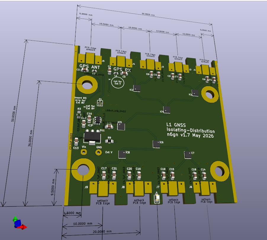
Note: 20 May 2026, There is a newer version 1.7 which has updated the original and provided less expensive and more available comonents.
However, this has not yet been built and tested.
A KiCad archive of this newer version which includes both Source Files and Kit Files (in the 'Production' Directory) which may be directly dropped onto the JLCPCB PCB web page for manufacture. The .zip file is Gerbers for the bare PCB, the .bom and.pos files are for bill of materials and positioning which are dropped onto the JLCPCB PCBA pages which follow.
|
||||
Description |
Provider |
Source Code |
Notes |
Approximate Material Cost(excludes setup fees and shipping) |
AssembledGNSS PCB |
Download PCBKit Files |
DownloadSource Files |
Use
Newer v1.7 KiCad Project
Archive Instead. Kit files are in 'Production' folder and may be
dropped directly onto JLCPCB pages for fabrication. |
US$30 v1.7 design ~$10/board in quantity. |
Enclosure |
eBay |
US$6 |
||
EnclosureFront Panel |
DownloadFront PanelKit Files |
DownloadFront Panel Source Files |
US$1 | |
EnclosureRear Panel |
DownloadRear PanelKit Files |
DownloadRear Panel Source Files |
US$1 | |
Donation © 2023 n6gn