This is an injection locked
PLL for use with the RX888 v2. It is one that I think has some
advantages over simple injection of an external clock. It
provides automatic switching between undisciplined/internal and
disciplined/external reference operation, can provide sub-ppb
frequency accuracy and low spurious and spectral noise power density
clocks forthe ADC. It has an advantage that even if there is an
interrupted connection with an external disciplining source, perhaps
because of a cable or a frequency change, the RX888 will NOT lose a
clock which can cause a host SDR program to crash and require complete
restart. The automatic switching within this PLL will simply
cause the free-running but settable frequency of its VCXO to be used
until the break is restored.
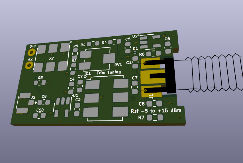
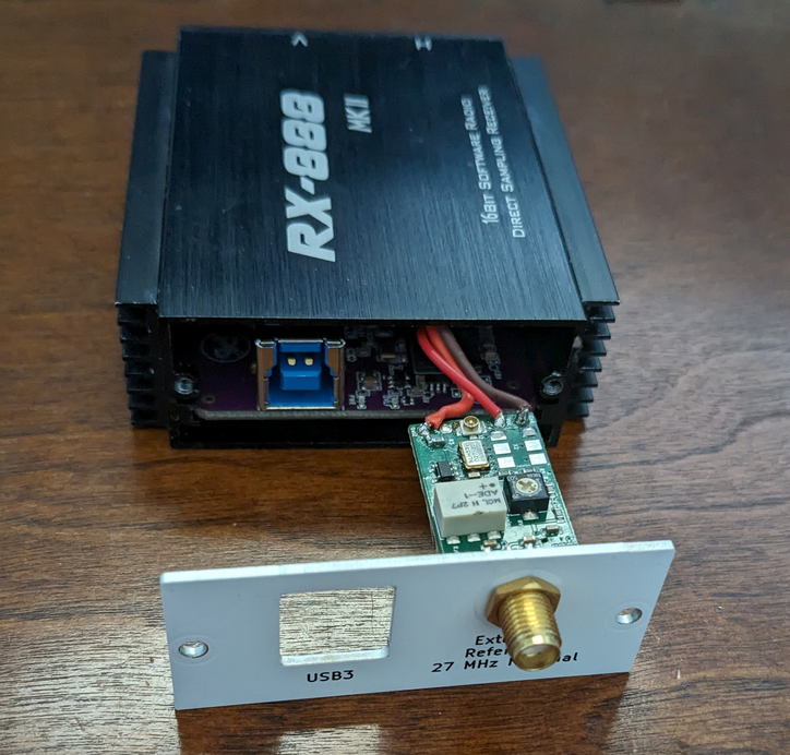
It is in the form of an add-on PCB
that can mount inside an RX888 as shown below. It
uses a Type I PLL and replacement VCXO to replace the OEM
one.


For
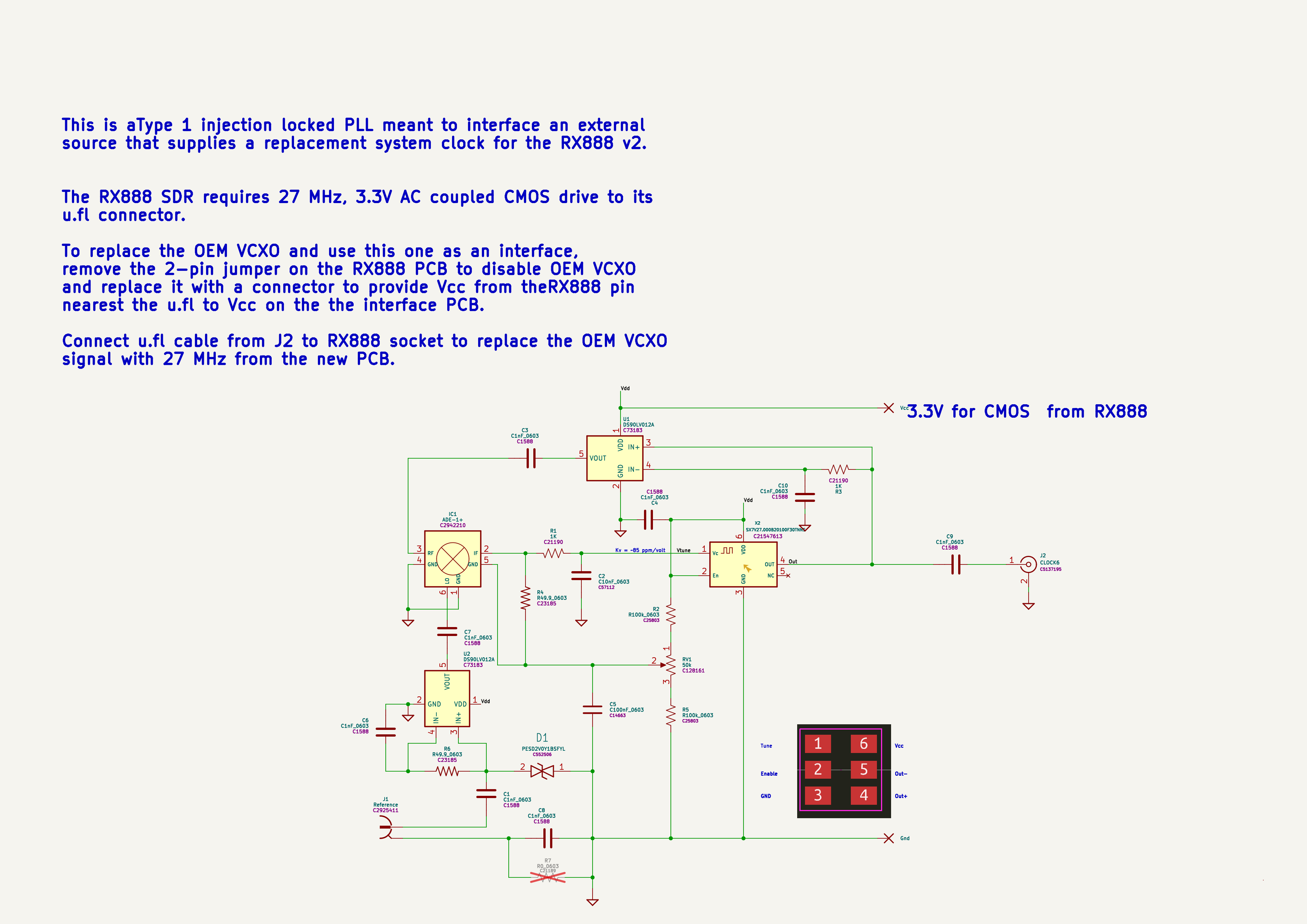
better quick viewing of the design, download the Source
file from the Material
List below , unzip it and drop the .sch or .pcb file onto kicanvas from a web browser.
[Caution]
Many installations will require internal soldering
probably in an SMD environment.
This may beyond what many should choose to attempt !
In the RX888 it is possible to
install it without any soldering but does require connecting a u.fl
cable to the connector on the RX888 PCB. This itself may be difficult,
u.fl connectors can be tricky. It receives 3.3V power from the 3 pin
jumper/header inside the Rx888. The jumper is replaced with a
connector that provides a single connection the Vcc on the new PCB.


Frequency trimming is provided by
the potentiometer on the PCB which sets unlocked/undisciplined
operation close to 27.0000 MHz. When an external 27 MHz
reference signal of -15 to +15 dBm is injected at the SMA, the PLL
"turns on" to phase lock the VCXO to the external reference
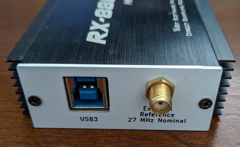
frequency. The external input terminal is DC blocked and even the
shield can be completely isolated to greatly reduce common mode
current. The selection of shield ground or isolation is done with a
lock washer on the inside when the board is installed. The SMA
connections presents 50 ohm impedance to the driving external
reference so that when normal 50 ohm coaxial cable is used the
shape of the reference signal is maintained.
|
||||
Item Description |
Provider |
Source Code |
Notes |
Approximate Material Cost(excludes setup fees and shipping) |
Assembled IPLL PCB |
Download IPLL Kit Files |
Download IPLL Source Files |
US$15 | |
| u.fl cable for RX888 use | Amazon | 2" cables are available but make it difficult to slide PCB in/out, use 6" | ||
RX888 Rear Panel |
Download Rear Panel Kit File |
RX888 Rear Panel Source Files |
||